74ls173 Circuit Diagram
74ls11 triple 3 74ls165 circuit diagram. Ram memory circuit bit cell binary watson circuits figure latech edu
74LS165 circuit diagram. | Download Scientific Diagram
How do i make a 74ls170 or 74ls670 register file reliably clock in data Renu kanwar: bcd to 7 segment decoder Pinout ic datasheet output configuration
Decoder segment bcd 7447 ic display 74ls47 datasheet 7446 driver 7segment using circuit gate logic pdf pins connected solution cant
Data and instruction registers — sap-1 processor architecture documentation74ls173 4-bit d-type registers ic with 3-state output Sap instructionEdge reliably tried talks circuits inverter detection.
.
![[SOLVED] - 3-digit Frequency Counter | Forum for Electronics](https://i2.wp.com/obrazki.elektroda.pl/4938747500_1366114212.jpg)

74LS11 Triple 3 - Input AND Logic Gate IC - Datasheet

74LS165 circuit diagram. | Download Scientific Diagram
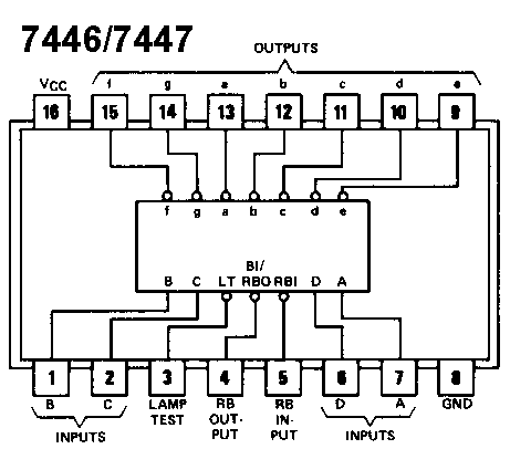
Renu Kanwar: BCD to 7 segment Decoder

How do I make a 74LS170 or 74LS670 register file reliably clock in data

Watson

Data and Instruction Registers — SAP-1 Processor Architecture documentation

74LS173 4-Bit D-Type Registers IC With 3-State Output | Datasheet